


 Contact us
 How to find us


Integrated Circuit Design Platform
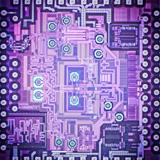
The Integrated Circuit Design Platform, located in MINATEC’s Advanced Components Building, boasts a team of 150 specialists developing architectures and digital, analog, mixed, and RF circuits on bulk and organic silicon and SOI. The team also includes embedded software specialists and works in conjunction with the embedded systems platform at the CEA’s Paris-Saclay campus.

The platform has a complete range of professional CAD tools like Cadence, Mentor Graphics, Synopsys, and Agilent, as well as emulation, testing, and characterization resources. It has an annual operating budget of €10 million.
The platform’s size and equipment make it the largest design center of its kind in Europe. It boasts world-class expertise in System on Chip (SoC) architectures, RF circuits and architectures, analog and mixed circuits and architectures for imaging circuits and sensor interfaces, thin SOI transistors, and new MOS, 3D assembly, and photonics-on-silicon concepts.
The platform’s activities include working with MINATEC labs and partners from industry as well as participating in research programs sponsored by ANR (the French National Research Agency), AII (the French National Industrial Innovation Agency), Eureka, FP7 (the EU Seventh Framework Programme), and competitive clusters. Some of these projects require the work of more than ten researchers per year for several years.
The circuits designed have a wide variety of applications in industries like telecommunications, automobile, multimedia, healthcare, and defense.
Contact: severine.vignoud@cea.fr
Thesis, Internship, Post-doc Offers
More