


 Contact us
 How to find us


Nanotec 300 Platform
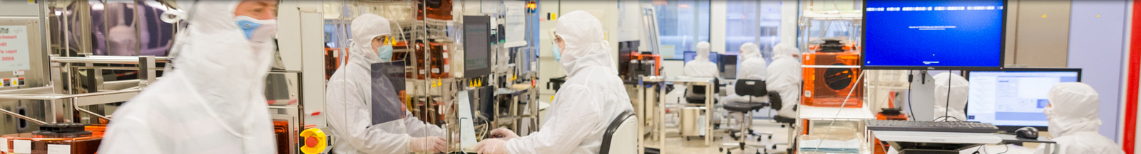
The Nanotec 300 Platform has a staff of 250 people working on the advanced microelectronics research needed for the substrates and sub 32 nm circuits of the future. The platform offers 5,000 square meters of clean room space with 300mm lithography, etching, depositing, implanting, and heat treatment equipment and the associated characterization equipment.
Building the microelectronic components of the future

The facility represents a total investment of more than €100 million to date. Using bare silicon wafers, the platform develops elementary processes and complete integration modules. Several million euros in new equipment investments are made each year.
Nanotec 300 also has access to the resources of the STMicroelectronicscampus in Crolles, just outside of Grenoble, and runs joint production with STMicroelectronics on short loops between the two sites. The platform also works with IBM in Albany, New York, and boasts several partnerships with academic researchers.
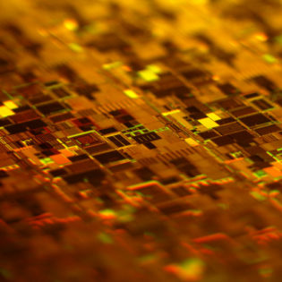
The work carried out at Nanotec 300 focuses on planar and 3D structures at the frontier of CMOS technology (More than Moore), as well as breakthrough technological processes. In addition to exclusive research programs run jointly with a select handful of partners from industry, the platform is also used for non-exclusive programs with semiconductor manufacturers, component makers, and vendors under the Joint Development Program.
Contact: gilles.simon@cea.fr
Thesis, Internship, Post-doc Offers
More