


 Contact us
 How to find us


A novel process to realize 4H-SiC nanowire arrays for biomedical applications
Published : 22 October 2019
SUJET STAGE Master 2 ou Projet de Fin d’Etudes:
A novel process to realize 4H-SiC nanowire arrays for biomedical applications
The arrays of vertical nanopillars and nanowires (NW) are highly interesting for various applications. Such arrays are natural candidates for two-dimensional photonic crystals.In addition, the pitch between pillars could influence biological cell adhesion. A pillar structure in a microfluidic system, with a flow passing orthogonally to the pillar direction, may function as a size filter for molecules. Moreover, the vertical nanowire arrays are an electronics architecture combining a scalable and reproducible structure with good electrical performance.
SiC nanowires are of high interest since they combine the physical properties of SiC with those induced by their low dimensionality [1 ].
The previous efforts to form top-down vertical SiC by plasma etching suffered from the gradual increase in the rate of the lateral etch of the hard-mask that resulted in a pyramidal shape [2 ].
A new method resolving the above issue and simultaneously relaxing the need for high-resolution lithography has been proposed by a consortium of French (LTM, IMEP-LAHC) and Greek (FORTH) labs [3 ].
Initially, NIL (nanoimprint lithography) has been employed for defining the nanopillar network. NIL is in many respects capable of producing results comparable to those of e-beam lithography, but at a considerably lower cost and with a much higher throughput.
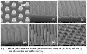
More details on the NIL steps are described in [3]. Then, hard mask etch instead of lift-off has been employed for obtaining vertical hard mask sidewall. Finally the diameter of the nanopillars has been reduced by sacrificial oxidation down to 80nm.
Initial results of photoluminescence have exhibited a decrease of FWHM of band-to- band recombination when the nanowire diameter is reduced. Nevertheless, quantum effects related to carrier confinement due to small dimensions have not been observed. Towards this aim the diameter of the initial pillars formed by the NIL technique has to be lower or close to 100nm in order to get after sacrificial oxidation arrays of NWs with diameter lower than 10nm. Furthermore, initial SiC material should be a low-doped, high-crystalline one and not highly doped bulk substrates.
The planned work in the frame of the proposed internship will deal among others with the formation of a Si master stamp incorporating pillars of around 100nm. In the beginning of the work, simulation will be performed in order to define the minimum diameter, maximum height and minimal spacing, since the adhesion among nanowires is the factor that reduces the mechanical strength. Once the simulations will define the optimum NW network configuration, a Si master stamp will be fabricated by e-beam lithography. Then, soft working stamps will be fabricated from the master stamp. The latter will be used for the fabrication of SiC pillar arrays and subsequent experiments for sacrificial oxidation. A series of optimization experiments with feedback from characterization results will be realized.
The work will be performed at two MINATEC labs. All technological processes will be realized at LTM while physical characterization will be performed at IMEP-LaHC.
Continuation towards a PhD: ideal case
Contacts: Jumana Boussey (LTM – Grenoble): jumana.boussey@cea.fr
Konstantinos Zekentes (IMEP–LaHC – Grenoble): Konstantinos.Zekentes@grenoble-inp.fr
Duration of the intership : 6 months, around 550 Euros/month
References
[ 1] K Zekentes and K Rogdakis, J. Phys. D: Appl. Phys. 44 (2011) 133001
[2 ] J. H. Choi, L. Latu-Romain, E. Bano, F. Dhalluin, T. Chevolleau, T. Baron, J. Physics D, 45 (2012) 235204A.
[3 ] Maria Androulidaki, Maximilien Cottat, Antonios Stavrinidis, Cecile Gourgon, Camille Petit-Etienne, Edwige Bano, George Konstantinidis, Jumana Boussey, Konstantinos Zekentes, Book of abstracts MNE 2019, Rhodes, Greece, (September 2019)


