


 Contact us
 How to find us


Development, modeling and characterization of flexible transducers based on piezoelectric nanowires
Published : 7 November 2017
MASTER Student Training : First Semester 2018
Keywords:
Nanotechnologies, Nanowires, Piezoelectricity, Semiconductor Physics and technology.
Training:
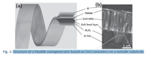
Very recently, the scientific community gets interested in nanowire devices, because of their unique electrical and mechanical properties due to their 1D structure. These properties could be exploited advantageously for several kinds of applications, such as sensors, actuators and energy harvesting devices (Fig.1)[1].
The training will mostly concentrate on the mechanical to electrical transduction using a composite material based on ZnO nanowires. These nanocomposites are expected to outperform thin piezoelectric films [2][3]. The purpose of this training is to evaluate the performance of the nanocomposites when integrated on flexible substrates.
The training has three different and correlated goals:
Participate to the fabrication of nanocomposite layers and triboelectric materials integrated on flexible substrates.
Characterize electromechanically the fabricated devices thanks to a specific test bench.
Participate to the modeling of piezoelectric nanocomposites using the Finite Element Method (FEM) approach.
The achievement of these goals will allows us to better understand the underlaying physics and phenomena involved and to improve the performances of the composite material or triboelectric devices for energy harvesting or sensing applications.
The student will benefit from an established collaboration framework and will have the opportunity to contribute to national and European projects related to energy harvesting for autonomous systems.
This subject will be pursued on a PhD thesis.
References:
[1] S. Lee, R. Hinchet, Y. Lee, Y. Yang, Z.-H. Lin, G. Ardila, L. Montes, M. Mouis, Z. L. Wang, “Ultrathin Nanogenerators as Self-powered/Active Skin Sensors for Tracking Eye Ball Motion”, Adv. Funct. Mater., 24 (2014) p. 1163-1168.
[2] R. Tao, G. Ardila L. Montes and M. Mouis, “Modeling of semiconducting piezoelectric nanowires for energy harvesting and sensing” Nano energy, 14 (2015) p.62-76.
[3] R. Tao, M. Parmar, G. Ardila, P. Oliveira, D. Marques, L. Montès, M. Mouis, “Performance of ZnO based piezo-generators under controlled compression”, Semiconductor Science and Technology, 32(6) (2017) p. 064003.
More info:
Duration: 4 to 6 months (first semester 2018)
Level: Master 2 (or Master 1) / Engineering School
Location: IMEP-LaHC / Minatec / Grenoble, France
Advisor: Gustavo Ardila
About the laboratory:
IMEP-LAHC / MINATEC / Grenoble
IMEP-LAHC is located in the Innovation Center Minatec in Grenoble. The main research areas concern Microelectronic devices (CMOS, SOI, …), Nanotechnologies, Photonic and RF devices. It works in close partnership with several industrial groups such as ST-Microelectronics, IBM, … and platforms such as LETI, LITEN, IMEC, Tyndall. The training will be within the group working on MicroNanoElectronic Devices / Nanostructures & Nanosystems. The trainee will have access to several technological (clean room) and characterization platforms.
Contacts:
Gustavo ARDILA ardilarg@minatec.grenoble-inp.fr +33 (0)4.56.52.95.32


