


 Contact us
 How to find us


Simulation, development and characterization of transducers based on piezoelectric nanowires
Published : 12 October 2020
Master Student Training:
Period: first semester 2021
Simulation, development and characterization of transducers based
on piezoelectric nanowires
IMEP-LaHC / LMGP/ MINATEC / Grenoble-France
Keywords:
Nanotechnologies, Nanowires, Piezoelectricity, Semiconductor physics, Characterization, FEM simulation.
Training:
Very recently, the scientific community gets interested in nanowire (NW) based devices, thanks to their unique electrical and mechanical properties due to their 1D structure. These properties could be exploited advantageously for several kinds of applications, such as sensors, actuators and energy harvesting devices (Fig. 1) [1]. Moreover, the device performance is strongly affected by different parameters: NW density, dimensions, surface state and doping level, between others [2].
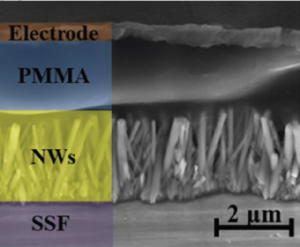 Fig. 1: Structure of a piezoelectric nanogenerator based on ZnO nanowires.
The training will mostly concentrate on the mechanical to electrical transduction using a composite material based on ZnO NWs. These nanocomposites are expected to outperform thin piezoelectric films [3][4].
The objective of this training is to develop piezoelectric nanocomposites based on ZnO NWs grown by metal-organic chemical vapor deposition (MOCVD) [5]. This technique allows the growth of NW arrays with a high structural and optical quality over a large range of substrates including silicon. The NWs will be characterized using SEM, XRD, AFM and other conventional techniques with the aim to reveal and control the surface states in these objects. The fabricated devices will be characterized using specific test-benches.
The training has four different and correlated goals:
- Participate to the growth of NWs by MOCVD.
- Participate to the fabrication of nanocomposite on silicon.
- Characterize electromechanically the fabricated devices thanks to a specific test-bench.
- Eventually, the student could participate to the modeling of piezoelectric nanocomposites using the Finite Element Method (FEM) approach.
The achievement of these goals will allows us to better understand the underlying physics and phenomena involved and to improve the performances of the composite material for energy harvesting or sensing applications.
The student will benefit from an established collaboration framework between LMGP and IMEP-LaHC laboratories (project ANR SCENIC 2021-2024 including also C2N and GEEPS laboratories). It will be possible to continue this subject in a PhD Thesis.
References :
[1] S. Lee, R. Hinchet, Y. Lee, Y. Yang, Z.-H. Lin, G. Ardila, L. Montes, M. Mouis, Z. L. Wang, “Ultrathin Nanogenerators as Self-powered/Active Skin Sensors for Tracking Eye Ball Motion”, Adv. Funct. Mater., 24 (2014) p. 1163-1168.
[2] R. Tao, M. Mouis, G. Ardila, “Unveiling the Influence of Surface Fermi Level Pinning on the Piezoelectric Response of Semiconducting Nanowires”, Adv. Electron. Mater., 4(1), (2018) p. 1700299.
[3] R. Tao, G. Ardila L. Montes and M. Mouis, “Modeling of semiconducting piezoelectric nanowires for energy harvesting and sensing” Nano energy, 14 (2015) p.62-76.
[4] R. Tao, M. Parmar, G. Ardila, P. Oliveira, D. Marques, L. Montès, M. Mouis, “Performance of ZnO based piezo-generators under controlled compression”, Semiconductor Science and Technology, 32(6) (2017) p. 064003.
[5] Q. C. Bui, G. Ardila, E. Sarigiannidou, H. Roussel, C. Jiménez , O. Chaix-Pluchery, Y. Guerfi, F. Bassani, F. Donatini, X. Mescot, B. Salem, V. Consonni , ”Morphology Transition of ZnO from Thin Film to Nanowires on Silicon and its Correlated Enhanced Zinc Polarity Uniformity and Piezoelectric Responses”, ACS Applied Materials & Interfaces, 12(26), (2020), p. 29583-29593.
More info:
Duration: 4 to 6 months (first semester 2021)
Level: Master 2 / Engineering School
Location: IMEP-LaHC /LMGP/ Minatec / Grenoble, France
Advisors: Gustavo Ardila (ardilarg@minatec.grenoble-inp.fr)
Vincent CONSONNI (vincent.consonni@grenoble-inp.fr)
About the laboratory:
IMEP-LAHC / MINATEC / Grenoble
IMEP-LAHC is located in the Innovation Center Minatec in Grenoble. The main research areas concern Microelectronic devices (CMOS, SOI, …), Nanotechnologies, Photonic and RF devices. It works in close partnership with several industrial groups such as ST-Microelectronics, IBM, … and platforms such as LETI, LITEN, IMEC, Tyndall. The training will be within the group working on MicroNanoElectronic Devices / Nanostructures & Nanosystems. The trainee will have access to several technological (clean room) and characterization platforms.
LMGP / MINATEC / Grenoble
LMGP is located in the Innovation Center Minatec in Grenoble and cover activities in (nano)-materials science including their synthesis by chemical deposition and their structural characterization. The training will be within the team “Nanomaterials and Advanced Heterostructures”.
Contacts:
Gustavo ARDILA ardilarg@minatec.grenoble-inp.fr +33 (0)4.56.52.95.32
Vincent CONSONNI vincent.consonni@grenoble-inp.fr +33 (0)4.56.52.93.58


