


 Contact us
 How to find us


Theory, design methodology and experimental validation of distributed amplifiers in advanced silicon technologies
Published : 17 May 2018
![]() PhD POSITION
PhD POSITION  Theory, design methodology and experimental validation
of distributed amplifiers in advanced silicon technologies
Laboratory: Research will be done at the RFIC-Lab (under creation)
Supervisor: Antonio Souza, Florence Podevin & Sylvain Bourdel
Phone: +33 4 56 52 95 67
E-mail: antonio.lisboa-de-souza@grenoble-inp.fr
Objectives:
Distributed amplifiers are of main concern in systems requiring very high gain-bandwidth products. At millimeter-wave frequencies, parasitic elements of lumped components become hard to model and control, while standard transmission lines are bulky and offer a limited flexibility in terms of characteristic impedances above 50 Ohm. To circumvent those restrictions, the PhD student will evaluate the use of a new kind of high impedance transmission line in distributed amplifiers, aiming to improve the amplifier´s gain-bandwidth product, matching and design flexibility. Taking into account aspects such as DC power, stability, Noise Figure and fabrication dispersion, the PhD student will propose an experimentally validated design methodology underlining the main tradeoffs that can be encountered in CMOS or BiCMOS technologies.
Context for millimeter-wave distributed amplifiers:
Mobile data transfer has exploded with the deployment of 4G and with the new needs created by this technology. According to Cisco´s Global Mobile Data Traffic Forecast Update 2016-2021, the annual Global IP traffic reached 1.2.1021 bytes in 2016, and will reach 3.3.1021 bytes in 2021. To address this demand, millimeter-wave systems (30-300 GHz) are required and so highly performing circuits at such frequencies. Especially, 5G working groups plan to aggregate a large number of physical channels to highly increase the effective data rate of mobile devices. When dealing with very high frequencies, distributed approach for active circuits is a well suited solution. Distributed systems allow the combination of a large number of channels, thus increasing the available bandwidth and hence the bit rate. This research area becomes a strategic field for the achievement of ultra-wideband communication systems. Traditionally, distributed circuits were dedicated to high cost wireline applications and designed using expensive technologies. The high performance of recent commercial CMOS/BiCMOS technologies now allows designing distributed circuits at low cost and could be a solution for the next generation of communication systems. In addition, specific techniques have been developed to reduce the size and increase the performance of passive circuits. Such techniques are very promising and surface efficient in modern CMOS/BiCMOS technologies. Moreover they also enable easy tuning capabilities of the passive circuits which are useful in the design of distributed circuits.
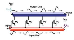
The research work consists in exploring the architecture of a transmission-line based distributed amplifier to be integrated into a standard CMOS/BiCMOS technology. A simplified illustration of a distributed amplifier is shown below. It is based on 2 propagation lines coupled by the transconductances of the transistors. The signal is amplified at each section of the input line and combined in the output line. Such structure can reach more than 100 GHz bandwidth in standard CMOS technologies.
Description of the Research Work:
The design of wideband distributed circuits requires the development of skills in the fields of passive circuits design (transmission lines, matching, electric and magnetic fields mapping, …) and also in active circuits design (PAs, oscillators, LNAs, …). This study will be based on the expertise developed in the laboratory in the field of active millimeter-wave circuits and innovative devices using slow-wave techniques. In this study, the input and output line of the amplifier will be designed considering different kinds of transmission lines.
A preliminary study has already been carried out and a first architecture has been recently proposed with an original design methodology, to be fabricated in July 2018. This approach is quite new and appears to be very promising in this research field that suffers from a lack of design/optimization methodologies. Quite unusual, the student will have the opportunity to characterize this circuit at the early beginning of his PhD thesis, what will strongly guide and help him in designing further circuits. Based on this preliminary study, the student will have to make a state of the art on the following topics: low-loss transmission lines, high frequency gain boosting methods for active cells, stability enhancement techniques, architectures and layout-oriented design for (distributed amplifier) compact circuits. The PhD student will then develop new types of distributed amplifier based on specific transmission lines (slow waves eventually), or by fully distributing the transconductances all along the transmission lines. The performance comparison will help to demonstrate the proposed ideas. During the PhD, the student will develop skills on:
– passive circuits by using the tools and expertise available in the laboratory to design passives;
– on active circuits linear and non-linear analysis; instrumentation and measurement, by using the laboratory infrastructure to characterize the circuits developed.
The work will be based on recent CMOS/BiCMOS technologies, such as the 55-nm BiCMOS technology of ST-Microelectronics, which is a quite innovative technology dedicated to millimeter waves applications.
Skills: Cadence, ADS, HFSS, Scilab or Matlab, Active and Passive RF circuits
This work will be performed in partnership with the Federal University of Paraiba (UFPB), Brazil, and some travels may be envisaged between University Grenoble-Alpes and UFPB.
Please send a CV and motivation letter (preferred before 5th of June) to: antonio.lisboa-de-souza@grenoble-inp.fr


