


 Contact us
 How to find us


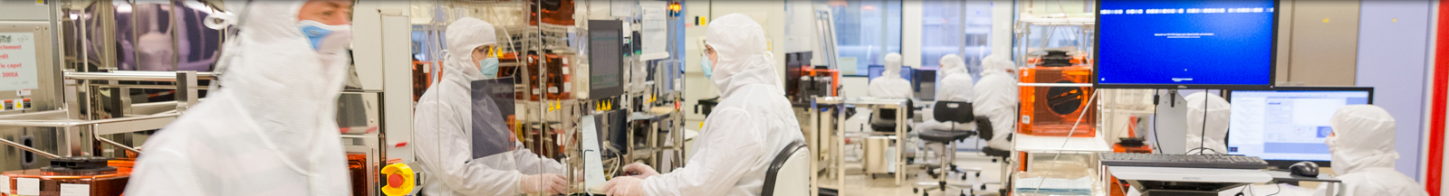
Research: 2021 year in review
 Quantum supremacy still not a given
Nature published Google’s groundbreaking results on a 54-qubit quantum computer in October, effectively declaring that quantum supremacy had been achieved. A few weeks later, however, a team of researchers from Irig and the US-based Flatiron Institute produced very similar calculations on a common laptop computer.
Google did reach an impressive milestone when it successfully operated a “real” quantum machine with 54 physical qubits. The tech giant’s researchers performed a calculation that even the best conventional machine would have taken 10,000 years to do, in just 200 seconds. One thing the research did not factor in, however, is this: Because of the quantum computer’s inherent precision and decoherence problems, the error rate of each operation is 1%.
Multiplying the number of qubits should not be the end goal
The Irig-Flatiron Instituteresearchers posited that Google’s machine did not even come close to utilizing the full power of quantum. They then used quantum-state compression algorithms to simulate the Google machine’s actual operation…on a regular consumer-grade computer! In just a few hours they completed the same calculations that the Google researchers said would take decades.
Their findings refocus attention on the real issue, which is not necessarily to build machines with more qubits, but rather to improve reliability—something that still raises serious theoretical and practical challenges. Another added bonus of the research is that Irig developed a tool unlike any other for evaluating the performance of current and future quantum computers. Irig has obtained several grants for further research on this topic.
Contact: xavier.waintal@cea.fr
For Intel and CEA-Leti the future is 3D
CEA-Leti and Intel, the world’s largest foundry, signed a contract expanding their partnership into 3D-integrated processors for high-performance computing via a multi-year R&D program in Grenoble.
Intel and CEA-Leti began working together on IoT and very-high-speed wireless communications in 2016. The company recently decided to expand its successful collaboration with CEA-Leti into one of its historic and most strategic markets, high-performance computing.
The race to achieve more compact and powerful HPC processors has spurred foundries around the globe to make sustained R&D investments in advanced technologies. The industry giants are currently working on technologies at the 14 nm and 10 nm nodes; 7 nm and, possibly, 5 nm, are further away. But as the technology gets smaller, each step forward is slower and costlier. 3D integration, which entails vertically stacking chips inside a device, adds even more complexity.
All roads lead to 3D
Intel and the CEA, through its institutes CEA-Leti and CEA-List, have strikingly similar 3D roadmaps. To improve bandwidth and reduce power consumption, both partners have opted to use active interposers to interconnect physical layers like processors, memory, and RF components. Additionally, CEA-Leti has a solid reputation for its 3D integration research. The institute is already working on 3D integration (for other applications) for STMicroelectronics, for example, as well as for several OEMs. Some of this research is part of a CEA-Leti partnership with IRT Nanoelec.
With so much to offer, it is no surprise that CEA-Leti was Intel’s partner of choice for this new R&D program, which kicked off last September but was kept under wraps until the partners announced it publicly in December.
New SALD pen could improve deposition
Selective-area laser deposition, or SALD, offers the advantages of being fast and suitable for use on large surfaces. Researchers at LMGP have made SALD even better with a new innovation. They took advantage of the design flexibility offered by 3D printing to come up with customizable and affordable SALD injection heads. The pen-style SALD injection heads can be mounted on an XYZ machine to perform selective 3D chemical deposition of functionalized materials with no need for masks or a vacuum deposition chamber. Plus, in terms of resolution, the high-precision SALD pen deposits material exactly where it is needed (to within one millimeter laterally) and in the right amount (to within one nanometer in terms of thickness).
LMGP is currently engaged in an EU research project to improve lateral resolution to within a micron. This enhanced lateral resolution would expand the potential uses of the SALD pen into microelectronics, for example. The research was published in Advanced Materials Technologies.
Video showing the deposition of a circle of ZnO: https://onlinelibrary.wiley.com/action/downloadSupplement?doi=10.1002%2Fadmt.202000657&file=admt202000657-sup-0006-MovieS5.mp4
Contact: david.munoz-rojas@grenoble-inp.fr
April 2021
Silicon can emit single photons at 1.28 microns
Irig was among the partners on a French national research agency (ANR) project that resulted in the on-demand emission of single photons in silicon at 1.28 µm, a wavelength used in telecommunications. They did it by introducing carefully-engineered defects into the material. The goal is to integrate this photon source into CEA-Leti chips for quantum communications.
There is certainly no lack of research on point defects in silicon and, specifically, light-emitting defects formed by carbon pairs interacting with interstitial silicon atoms called G-centers. However, it had never been posited that these defects could emit single photons. The Octopus project implanted G-centers into the silicon and demonstrated that they could emit single photons. The findings were published in Nature Electronics.
A potential enabler of quantum communications
The G-center the researchers engineered turned out to be a very efficient source of photons that could potentially be embedded into chips. Using an external source to generate photons and then injecting them into the chip creates line losses. Single photons, however, are not affected by these reamplification issues.
The partners are now working with CEA-Leti to integrate the G-center into a chip to assess its potential for quantum communications. They are investigating the degree of spin freedom of isolated G-centers embedded in membranes of silicon 28, a spinless isotope. The G-center could be a future single-spin quantum memory, capable of storing the state of a single photon.
Contact: jean-michel.gerard@cea.fr
Germanium-laser-on-silicon contacts could become more stable
Optronics researchers love the idea of germanium lasers on silicon—but the devices’ contacts are highly thermally unstable. In a world-first, a PhD research project being conducted at CEA-Leti has explained this unpredictable behavior. PhD candidate Andrea Quintero has published ten papers on the phenomenon over the past three years, even winning a Best Paper Award at ECS Prime 2020.
Germanium is an indirect gap material, so it must have tin content of 10% or 15% to deliver the desired optical performance. However, a heating process used to fabricate the contacts exposes them to temperatures that cause tin segregation. Andrea utilized several pieces of equipment at the Nanocharacterization Platform (PFNC) to observe and formally describe the diffusion of tin towards the surface of the material.
Go to the article: https://doi.org/10.1149/09805.0365ecst
Contact: camille.giroud@cea.fr
June 2021
Could neuroillumination be Clinatec’s new weapon against Parkinson’s disease?
Exposing degenerating neurons to near infrared light could slow the progression of Parkinson’s disease. A preclinical trial of this approach in 2016 produced excellent results. The first patient in a new clinical trial was implanted with the neuron-illuminating device at Clinatec at the end of March.
Parkinson’s disease affects 6.5 million people worldwide. Although treatments—like the deep brain stimulation invented by Dr. Alim-Louis Benabid in the 1990s—can temporarily alleviate the symptoms of Parkinson’s, there is currently no way to slow the progression of the disease.
A four-year trial on a cohort of fourteen patients
Developed by Grenoble-Alpes University Medical Center with university labs, the CEA, and Boston Scientific, the treatment is creating new hope now that clinical trials have started. Illuminating degenerating neurons with near infrared (NIR) light has long-lasting biological effects, slowing down the once-irreversible process, which, if left unchecked, leads to the progressive loss of motor function in the patient.
Grenoble-Alpes University Medical Center’s Dr. Stéphan Chabardès, who also runs the medical unit at Clinatec, implanted the neuro-illumination probe in a 55-year-old female patient on March 24. The patient will be monitored for four years. Hospitals in Lyon, Marseille, and Créteil are helping to recruit the additional thirteen patients needed for the trial.
Contact: thierry.bosc@clinatec.fr
Lensless imaging could make phage therapy faster
Researchers from CEA-Leti, Irig, and LTM recently worked with a team in Lausanne* to develop a lensless device capable of reducing the time it takes to identify active phages on antibiotic-resistant bacteria at least threefold. The large-area image sensor (24×36 mm2) reads the optical signature of areas occupied by bacterial debris. The technique could be more effective than naked-eye observation and would result in fewer false negatives.
An ANR (France’s national research agency) priority program to develop the technique further is about to begin in conjunction with Hospices civils de Lyon, a major university medical center. According to the WHO, antibiotic-resistant infections could cause 10 million deaths per year by 2050, making phage therapy a strategic solution.
Contact: camille.giroud@cea.fr
Quantum: CMOS withstands very low temperatures
In the future, quantum devices cooled to 10 mK will be used together with conventional electronics. Which raises the question of how well CMOS components, designed to operate at ambient temperature, hold up in temperatures close to absolute zero. To test out this scenario, researchers from Irig and CEA-Leti made hybrid circuits with the two technologies.
First, they evaluated a conventional CMOS TIA, measuring currents in the picoA range. The circuit was able to withstand the cold, but its bandwidth was under 4 kHz.
The test was done on a 28 nm FDSOI circuit. To increase measurement speeds, improvements will have to be made to the design. As the research progresses, other CMOS circuits will be evaluated for quantum applications.
Contact: louis.jansen@cea.fr
October 2021
Making IoT devices more resilient to attacks
Currently, when an IoT device (a “node” on the network) is attacked by hackers, the entire network can be affected, as can internet-connected third-party infrastructure services.
A new solution called iMRC uses a control server to detect attacks and takes over any devices that have been compromised to find out what vulnerability the hackers used to get in so that a software patch can be sent out.
Developed by CEA-Leti, CEA-List, and Tiempo Secure, iMRC won a Grand Défi Cyber award from the French government.
The solution includes a secure physical element and an embedded supervision system that interacts with the control server.
It should be ready for production by the end of next year and will be of particular interest for critical systems for the energy industry, the medicine of the future, and transportation.
Contact: camille.giroud@cea.fr
Reversing magnetization with an electric field
Researchers at Irig working with colleagues in Romania* recently discovered that the magnetization of an MRAM-cell-type nanostructure can be reversed by applying an electric field rather than an electric current. Their results should lead to some exciting developments.
When an electric field is applied, the write speed is ten times faster and uses 100 times less energy compared to standard STT-MRAM. And, because Joule effect losses are reduced to a similar degree, the memory stack doesn’t get as hot, which is good news for STT-MRAM reliability and robustness.
Simulation was used to determine the optimal switching parameters, which were then confirmed experimentally.
The research, which is ongoing, could lead to the design of innovative components.
A patent has also been filed.
* Babes-Bolyai University and Technical University (Cluj-Napoca, Romania)
Contact: liliana.buda@cea.fr
December 2021
Material criticality comes into its own as a research topic
For the past three years, four Grenoble laboratories have been working together, using methods from materials science and economics to find alternatives to the critical materials in white LEDs.
Their work, funded by the UGA Idex grant, marks a departure from conventional technology research.
Scientists’ interest in the scarcity and criticality of certain materials is not new.
What is new is that they are treating them as research topics in and of themselves, and not just constraints to be factored into other research.
With CEA-Leti’s support, LMGP, Institut Néel, and applied economics lab GAEL have been investigating the rare and critical elements (gallium, indium, yttrium, and cerium) in white LEDs.
Consumers are willing to pay more
A PhD dissertation based on research at LMGP and Institut Néel pointed to zinc oxide nanowires and identified aluminoborates as a promising—and rare-earth-free—class of luminophores.
CEA-Leti, which possesses substantial know-how in LED systems, supported this research.
On the economic side, GAEL completed a study that revealed consumers would be willing to pay up to 30% more for white LEDs that are free from critical materials.
This cross-disciplinary research was financed by the UGA Idex grant through the CDP* Eco-SESA project.
The resulting PhD dissertation won a national C’Nano award.
The grant and award confirm that broader issues like how rare these minerals are, how they are mined, where they are sourced, and how well consumers accept them are just as at home in the debate as the materials’ technical properties.
*Cross Disciplinary Programs
Read the dissertation: https://www.sciencedirect.com/science/article/abs/pii/S1364032121001635
Contact: olivier.boulle@cea.fr
Larger defect-free graphene layers produced
Irig and ESRF recently attracted the attention of the global nanoelectronics community when they produced defect-free single-crystal graphene layers measuring several square millimeters. The tiny layers are a million times larger than the square micron commonly obtained until now! The researchers did it by growing the 2D material on liquid copper at 1,100 °C rather than on solid copper. Combining the reflection and diffraction measurements of synchrotron X-ray imaging, Raman spectroscopy, and optical microscopy, they were able to monitor and control the formation of the graphene crystals in real time. The layers obtained are as good as exfoliated graphene sheets, but they do degrade as the liquid copper solidifies, and must be separated before the substrate cools. The research was conducted under EU project DirectSepa, which has been running for a year now.
Learn more about DirectSepa: https://cordis.europa.eu/project/id/951943/fr and https://www.esrf.fr/home/news/spotlight/content-news/spotlight/spotlight392.html
Conact: gilles.renaud@cea.fr; maciej.jankowski@esrf.fr
Banking on SiC for neural interfaces
Silicon carbide, widely used in power electronics, could also be used in neural interfaces.
The new SiCNeural project, funded by the French National Research Agency (ANR) and coordinated by IMEP-LaHC, is investigating the question.
The project partners will develop a very thin (less than 10 microns) and flexible all-SiC neural electrode.
SiC is a biocompatible material with three phases—amorphous, polycrystalline, and monocrystalline—that the researchers intend to take full advantage of.
They will also nanostructure the material to increase the exchange surface and brain stimulation capacity.
Their goal is to overcome silicon electrodes’ short lifespans and tendency to cause inflammation.
Scientists from the Institut des Neurosciences in Grenoble will conduct in vivo proof of concept testing.
Learn more about SiC for biotechnology in this book (chapter 9 by IMEP-LaHC and LMGP): https://www.elsevier.com/books/silicon-carbide-biotechnology/saddow/978-0-12-802993-0
Contact: edwige.bano@grenoble-inp.fr
